At far infrared wavelengths, we use simple photoconductor detectors. Appropriate material is placed between two electrodes, actually thin metal films evaporated onto opposite faces of the material. A voltage is imposed across the electrodes. When the material absorbs light, it frees electrons (or solid-state "holes") and they drift under the electric field created by the voltage. The result is a tiny electric current, that must be sensed by the readout.
Arrays as large as 1024x1024 (and even larger if you have lots of money!) now exist for
the near and mid-infrared, generally buiolt along lines like our 24 micron array. Applying
this standard architecture to longer wavelengths is hard. First, long wavelengths imply
large pixel size that is not well-matched with a typical readout die size. Second, the
photoconductor needed for this wavelength (Ge:Ga) has a relatively low absorption
coefficient, and so the absorption thickness must be several millimeters. The standard
transparent-electrode configuration has poor charge collection efficiency for such
thicknesses. Finally, a far-infrared detector must be cooled to very low temperatures to
have adequate dark current performance. In standard arrays, the readouts (which are bonded
to the photoconductor) are a source of heat between the detector and the cold sink.
The Ge:Ga focal plane array is composed of 4x32 modules, whose design addresses these issues. The photons enter the detectors through optical concentrators. The detectors themselves are edge on, with a length of 2mm in the direction the photons are traveling but a thickness of only 0.5mm between the electrical contacts. This geometry maintains a large field in the detector material, for good charge collection, but it also allows for a long absorption length and high quantum efficiency. The detectors are mounted on thin sapphire sheets. The readouts (4 per module) are mounted on a multilayer ceramic board separate from the detectors so the power that must be dissipated in the electronics can be conducted away from the detectors, keeping them as cold as possible. The Hughes CRC-696 readouts were specifically developed for use with far-infrared detectors and have excellent low-temperature (below 2K) performance. They also include electrical feedback to maintain the bias voltage across the detectors precisely as signal is accumulated. Finally, the entire structure is mounted on a molybdenum frame; the material for the frame was selected to give good thermal conductivity and to have thermal expansion matched closely with the sapphire and the ceramic board. |
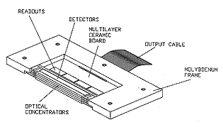 |
| An important "feature" of this type of array is that the images come in from the side. We can hide all the structure in the array behind the detectors, so that the array makes an image with no dead spots. We found it most practical to manufacture the array in sections, each of which is 32 detectors ("pixels") long and 4 pixels high. We then stack eight of these sections to make a completed 32 x 32 pixel array. | 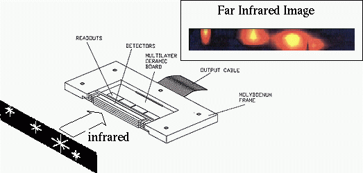 |
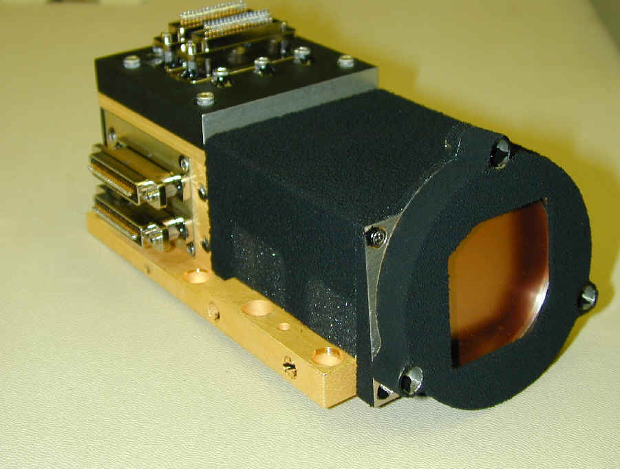 |
Here is the resulting array. The detectors themselves are hidden behind an
optical filter at the right side of the picture. Light passes through this filter and to
the detectors, where it is absorbed, the resulting currents are sensed with the readouts,
and the amplified signals sent out on a flex cable. This cable plugs into a larger one
hidden in the back part of the array (left side of the picture), and the latter cable
carries the signals to the output connectors. The input voltages and control signals are
also brought in through these connectors and cables. It was an exciting day when we delivered this array to Ball Aerospace to mount in the instrument!
|
To learn a lot more about this array, check it out here.
 |
|
|