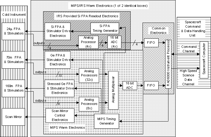
The warm electronics are shared with the IRS. These combined electronics provide circuitry for control of the three detector arrays, the scan mirror, and other cold instrument functions. In addition, they digitize the science and housekeeping signals and include a RAD6000 processor for data processing and formatting. The RAD6000 also receives commands from the spacecraft computer and sends formatted science and engineering data to it for compression and telemetry to Earth.
The MIPS/IRS warm electronics are designed to be standby redundant; that is, two identical electronics boxes are flown; both boxes are connected to the arrays and scan mirror in the cold instrument, but only one box is powered at a time. The electronics are housed in two identical ten slot chassis. The outside dimensions of each enclosure are approximately 340mm x 320mm x 204mm and the weight of each populated box is about 20Kg. Power dissipation of the electronics is about 45 watts. The electronics enclosure is designed to provide radiation shielding of the electronic components. The components themselves are also selected to be radiation hard. The diagram below shows the overall structure of the electronics.
A total of 40 identical analog chains (see on the right) are provided in the MIPS warm
electronics for the two Ge FPAs: 32 for the 70micron FPA and 8 for the 160micron one. The
cable connecting the FPA outputs to the MIPS warm electronics is over three meters long.
Since this cable is routed from the 1.5K instrument out to the 300K warm electronics box,
a low thermal conductivity wire is used for these conductors. Each cable contains 24 pairs
of twisted pair manganin wire protected by an outer shield; 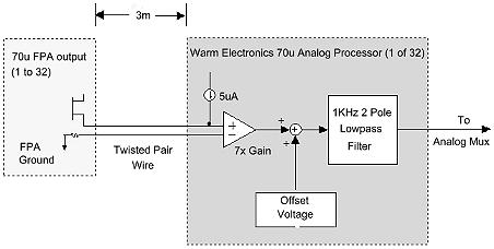 each output signal is twisted with a complementary ground
reference. The total capacitance of up to 700pF must be driven by the array output
amplifiers. An instrumentation amplifier in the warm electronics, which helps reject
common mode noise on the incoming signal and ground reference lines, receives the signals.
The output of the instrumentation amplifier is summed with a DC offset voltage and then
fed into a 1KHz two pole filter. The bandwidth of this filter was chosen to be low enough
to limit the FPA noise bandwidth and yet provide a reasonable readout time for the FPA.
The outputs of the 40 analog chains are multiplexed down to a single analog line, which is
fed to the analog to digital converter (ADC) as shown in Figure 6. A 16 bit ADC is used to
digitize the processed pixel data from the germanium FPAs. The overall Ge FPA signal chain
has a gain of 7x. Only 14 bits of the available 16 bits are processed. 14 bits (~20
electrons per ADU) provides good sampling of the FPA read noise, full coverage of the full
detector dynamic range and some margin to allow for mismatch between the DC outputs of the
various FPA readouts.
each output signal is twisted with a complementary ground
reference. The total capacitance of up to 700pF must be driven by the array output
amplifiers. An instrumentation amplifier in the warm electronics, which helps reject
common mode noise on the incoming signal and ground reference lines, receives the signals.
The output of the instrumentation amplifier is summed with a DC offset voltage and then
fed into a 1KHz two pole filter. The bandwidth of this filter was chosen to be low enough
to limit the FPA noise bandwidth and yet provide a reasonable readout time for the FPA.
The outputs of the 40 analog chains are multiplexed down to a single analog line, which is
fed to the analog to digital converter (ADC) as shown in Figure 6. A 16 bit ADC is used to
digitize the processed pixel data from the germanium FPAs. The overall Ge FPA signal chain
has a gain of 7x. Only 14 bits of the available 16 bits are processed. 14 bits (~20
electrons per ADU) provides good sampling of the FPA read noise, full coverage of the full
detector dynamic range and some margin to allow for mismatch between the DC outputs of the
various FPA readouts.
The analog chain for the MIPS 24 micron array is similar to the Ge:Ga analog chain shown above. Four identical analog chains are provided for this array. A differential receiver provides common mode rejection for the incoming signal. A two-pole filter is used to limit the bandwidth of the incoming signal. The filter bandwidth for this array is set at 40KHz due to the higher pixel sampling frequency. Four separate ADCs are provided within the IRS electronics to digitize the pixel data. The digitized pixel data from the ADCs are merged and fed into the RAD6000 instrument processor.
A hardware timing generator is used to produce the clock signals for the two MIPS Ge:Ga arrays, synchronization signals for the MIPS Si:As array, and deflection waveforms for the scan mirror. Synchronizing signals are fed from the MIPS timing generator to the IRS timing pattern generator, which produces the actual Si:As array clocking patterns. Both of these timing generators are implemented in hardware with no real time intrusions required by the instrument processor. The MIPS flight software controls the operation of these timing generators through register writes. In operation, the MIPS germanium FPAs will be read out at a frequency of 8Hz and the Si:As array at 2Hz.
Drivers are provided in the MIPS electronics for the array calibration stimulator sources and the thermal anneal heaters. The timing generator produces the stimulator flash pulses, which are synchronized with the array readout. The thermal anneal heater timing is controlled directly by the instrument processor.
The CSMM is controlled by a type I analog servo system. The actual CSMM deflection angle is continuously monitored and compared with the commanded angle. The error signal between the actual and desired positions is integrated and used to drive the CSMM actuator. Mirror deflection commands are generated digitally by the timing generator and converted to an analog command using a digital to analog converter (DAC). The timing generator produces all the required CSMM deflection waveforms including chop waveforms and the sawtooth pattern required by the MIPS scan map mode. The higher currents required by the CSMM and by the array thermal anneal heaters are carried to the cold instrument over a cable constructed of phosphor bronze wire.
 |
|
|