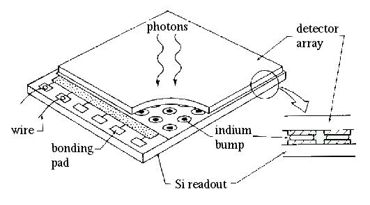
This array was developed under the leadership of the IRS team at Cornell, with processing by Boeing (formerly Rockwell). The Si:As arrays are "normal" direct hybrids, similar to the whole suite of infrared arrays developed over the last 15 years for use between 1 and 30 microns. They are made by fabricating both a grid of infrared detectors in a suitably optimized material, and also a silicon readout containing a grid of amplifiers. Indium bumps are evaporated on matching electrodes on these two grids. The detector array and silicon readouts are bonded by aligning the bumps and applying pressure; the mating bumps cold weld. When a bias is applied across the detectors, currents generated when photons are absorbed are conducted across the welded indium bumps into the input transistors of the readout amplifiers. The outputs of the amplifiers are multiplexed electronically in the readout and brought to bonding pads at the side of the device. Conventional wire bonding connects these points to pads in a chip carrier, and a similar set of wires carries service lines and clocks from the chip carrier contacts into the readout. See the figure below, from G. H. Rieke, "Detection of Light", Cambridge University Press (http://www.cup.org/) -- no library is complete without this book!
The devices MIPS will be using are described in more detail by Van Cleve
et al., "Evaluation of Si:As and Si:Sb Blocked Impurity Detectors for SIRTF and
WIRE", Proc. SPIE, 2553, pages 502 - 513 (1995).