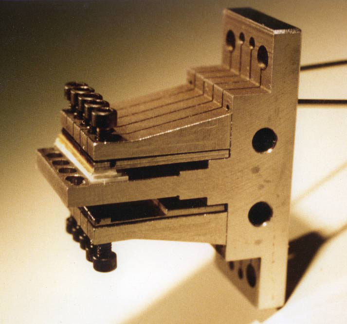
The way we have implemented stressed Ge:Ga detectors is shown in the figure on the right. A multi-fingered, double-sided clamp is made of very strong steel (Aermet 100), and five detectors are placed on each side of this clamp. Each detector can be stressed individually by tightening the screw on that detector's finger, bending the finger like a leaf spring. The stresses are distributed over the detector by a pressure plate, so it doesn't break. To make a full 2x20 array, we mount four of these 2x5 modules together, along with condensing cone feed optics to lead the photons into the detectors. See figure that illustrates the complete array with condensing cones and heat sink. The 160 micron array was built at the University of Arizona, with help from Lawrence Berkeley National Laboratory.
![]()