| When a semiconductor detector with a p-type impurity is put under stress,
it can detect lower energy photons than it could when unstressed. This surprising behavior
can be understood (with a little waving of the hands) because the photon must break bonds
in the detector to be detected, and if the detector is already under mechanical stress the
bonds are easier to break. This effect was first used in far infrared detectors by MIPS
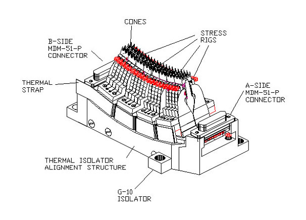
co-Is Eugene Haller and Paul Richards. The way we have implemented stressed Ge:Ga detectors is shown in the figure on the right. A multi-fingered, double-sided clamp is made of very strong steel (Aermet 100), and five detectors are placed on each side of this clamp. Each detector can be stressed individually by tightening the screw on that detector's finger, bending the finger like a leaf spring. The stresses are distributed over the detector by a pressure plate, so it doesn't break. To make a full 2x20 array, we mount four of these 2x5 modules together, along with condensing cone feed optics to lead the photons into the detectors. See figure that illustrates the complete array with condensing cones and heat sink. The 160 micron array was built at the University of Arizona, with help from Lawrence Berkeley National Laboratory. |
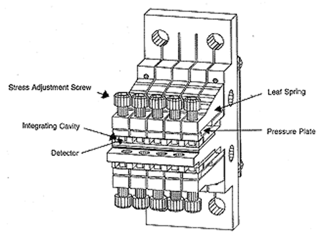 For a picture of a 2x5 module |
For a picture of the completed array
|
The flight array consists of four modules mounted together on a frame, but thermally isolated on fiberglass box members. A thermal strap goes to a heat sink at the side of the instrument, which is connected by a thermal strap to a button on the side of the helium vessel in the SIRTF cryostat. Because the stressing hardware takes a lot of room, we use reflecting cones to bring the light down onto the detectors. In this way, we have response over the full pixel area, not just in the center. |
| We built the array at the University of Arizona. Here is Rick Schnurr, carrying out the final assembly. | 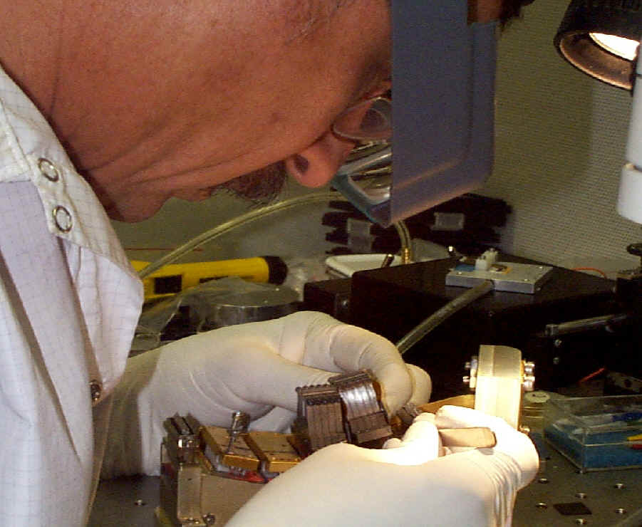 |
More than you probably ever wanted to know about this array is here.
 |
|
|